Advanced Micro Semiconductors Co., Ltd. (referred to as “AMSFAB” or “the Company”) announced today that the development of a series of photodetector process platforms, including MPD (Monitor Photodetector), 10G-25G PD (Photodetector) and 56G Pulse Amplitude Modulation 4-level (PAM4) PD, has been completed. The platforms, which feature high responsivity, high sensitivity, high speed and low dark current, provide low-cost, low-power, and efficient chip solutions for customers, which can be widely applied in fields including communication, industry, medicine and consumer electronics.
AMSFAB has a full range of advanced processes and specialty process solutions. The 10G-25G PD and MPD process platform based on indium phosphide (InP) materials adopts key processes of epitaxial growth, zinc diffusion, stepper lithography, and sidewall treatment. Photo receiver chips produced using the platform for GPON, XGPON and Combo PON OLT have a good match in electrical characteristics with circuits such as back-end trans-impedance amplifiers, in order to ensure sufficient conversion coefficient, linear range, signal-to-noise ratio, and fast dynamic response.

MPD
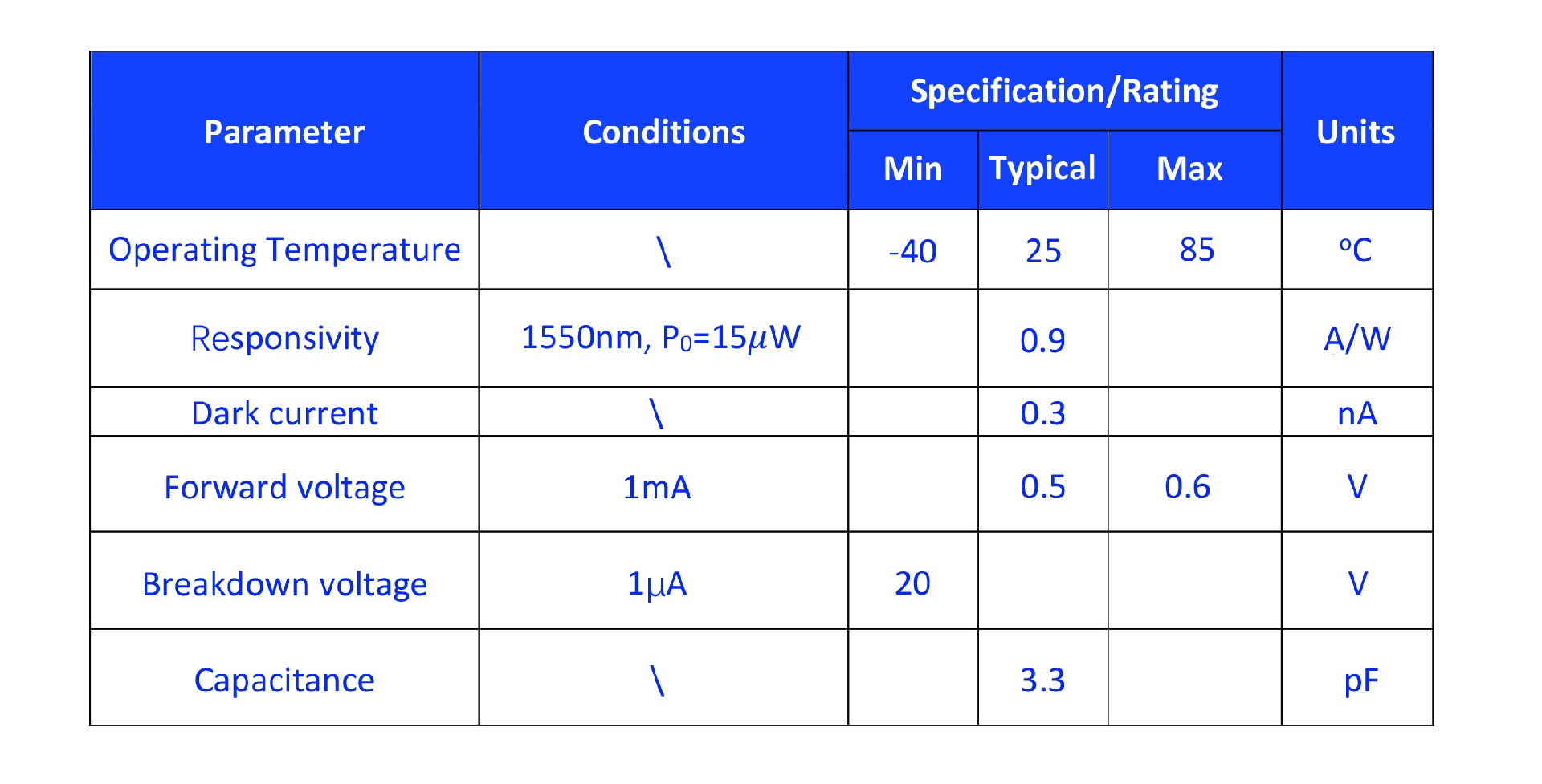
MPD optoelectronic characteristic parameters (T=25℃):


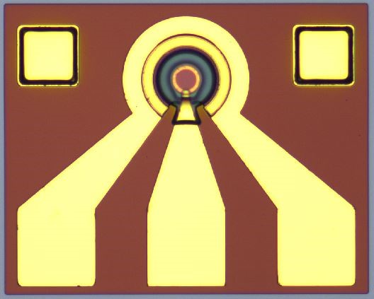
25G PD
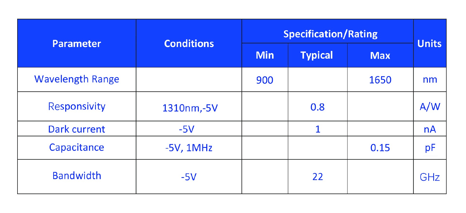
25G PD optoelectronic characteristic parameters (T=25℃):


56G PAM4
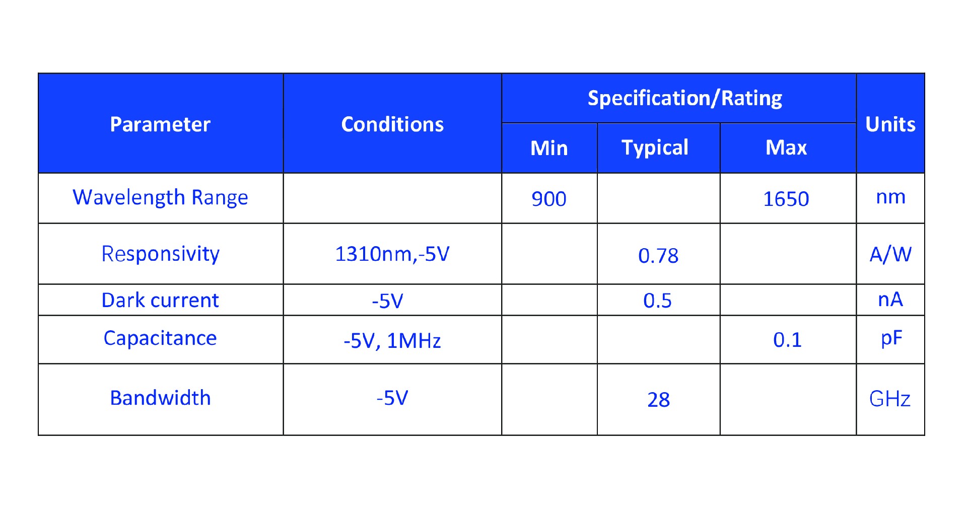
56G PAM4 optoelectronic characteristic parameters (T=25℃):

Through independent epitaxial R&D and the mass production process line, AMSFAB has also developed 3-inch and 4-inch InP-based detector epitaxial wafer process technology, zinc diffusion epitaxial wafer process technology, and the epitaxial wafer process technology for full-structure InP-based detectors with in-situ p-type doping, meeting the customers' requirements for customized epitaxial products in the fields of optical communication and sensing identification. Specifically, the 10G-25G PD 4-inch epitaxial wafer is the first 4-inch InP-based optoelectronic epitaxial wafer verified and developed by the 4-inch InP-based photonic chip mass production line in Chinese mainland.
In terms of product quality, AMSFAB has a holistic quality management system. From material management to the recording and testing of process flows, the Company has realized a full traceability of process flows. Together with the TO and module-level packaging test and the aging test system, the system ensures product consistency and process stability. AMSFAB also provides value-added services, such as design support and wafer testing, to shorten the time-to-market for customized products, thus creating greater business value for customers.
AMSFAB is committed to making product integration easier, saving costs, and reducing delivery cycles. We also have wafer-level testing ability for the dark current at high and low temperatures, bandwidth, and responsivity of PD/APD detectors. AMSFAB is on course to shift optoelectronic chip products from high-speed PD to high-speed and highly sensitive APD and optoelectronic receiver chips, fueling the infrastructure construction of the access network and transmission network.


